The Double Edge Flip Flop
Sometimes
it is necessary to use both the rising and the falling edge of the
clock to sample the data. This is sometimes needed in many DDR
applications (naturally). The double edge flop is sometimes depicted
like that:
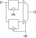
The most simple design one can imagine (at least me…), would be to
use two flip flops. One sensitive to the rising edge of the clock, the
other to the falling edge and to MUX the outputs of both, using the
clock itself as the select. This approach is shown below:
What’s wrong with the above approach? Well in an ideal world it is
OK, but we have to remember that semi-custom tools/users don’t like to
have the clock in the data path. This requirement is justified and can
cause a lot of headaches later when doing the clock tree synthesis and
when analyzing the timing reports. It is a good idea to avoid such
constructions unless they are absolutely necessary. This recommendation
applies also for the reset net - try not combining the reset net into
your logic clouds.
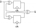
Here is a cool circuit that can help solve this problem:
I will not take the pleasure from you of drawing the timing diagrams yourself ![]() and realizing how and why this circuit works, let me just say that IMHO this is a darn cool circuit!
and realizing how and why this circuit works, let me just say that IMHO this is a darn cool circuit!
Searching the web a bit I came across a paper which describes practically the same idea by Ralf Hildebrandt. He names it a “Pseudo Dual-Edge Flip Flop”, you can find his short (but more detailed) description, including a VHDL code, here.
Powered by ScribeFire.


No comments:
Post a Comment